Types of MOSFET
MOSFET Structure and Symbol
The construction of the Metal Oxide Semiconductor FET is different from Junction FET. Both the Depletion and Enhancement type MOSFETs use an electrical field generated by a gate voltage to change the flow of charge carriers, electrons for n-channel or holes for P-channel. The gate electrode is placed on top of a very thin insulating layer and there is a pair of small n-type regions just under the drain and source electrodes.
As we study in the previous tutorial that the gate of a junction field effect transistor, JFET must be biased in such a way that it creates a reverse-bias of the PN-junction but in case of insulated gate MOSFET device no such limitations apply so here in MOSFET it is possible to bias the gate of a MOSFET in either, positive (+ve) or negative (-ve) polarity. Because of these features, this makes the MOSFET device very useful as electronic switches or to make logic gates because with no bias they are normally non-conducting and this high gate input resistance it means that very little or no control current is required as MOSFETs are voltage controlled devices.
MOSFETs are available in two basic forms,
- Enhancement-type
- Depletion Type
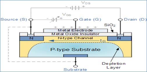
Depletion-mode MOSFET
The Depletion-mode MOSFET, is generally a switched “ON” (conducting) mode without the application of a gate bias voltage. Here is the channel conducts when VGS = 0 making it a “normally-closed” device it is not commonly used as compared to enhancement type MOSFET. For the n-channel depletion MOSFET, a negative gate-source voltage, -VGS will deplete the conductive channel of its free electrons switching and making the transistor “OFF”. Similarly for a p-channel depletion MOSFET a positive gate-source voltage, +VGS will deplete the channel of its free holes turning it “OFF”.
Here we conclude that, for an n-channel depletion mode MOSFET, +VGS means more electrons and therefore more current. Whereas
-VGS means fewer electrons and less current. The opposite is also applicable to the p-channel types.
Depletion-mode N-Channel MOSFET and circuit Symbols and Characteristics
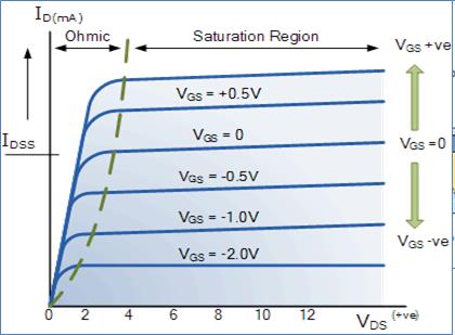
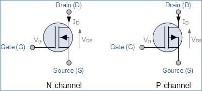
The depletion-mode MOSFET is constructed in the same way to their JFET transistor counterparts were the drain-source channel is inherently conductive with the electrons and holes already present within the n-type or p-type channel. This doping of the channel produces a conducting path of low resistance between the Drain and Source with zero Gate bias.
Enhancement-mode MOSFET
The more common Enhancement-mode MOSFET or eMOSFET, is the reverse of the depletion-mode type. Here the conducting channel is lightly doped or even undoped making it non-conductive. This results in the device being normally “OFF” (non-conducting) when the gate bias voltage, VGS is equal to zero. The circuit symbol shown above for an enhancement MOS transistor uses a broken channel line to signify a normally open non-conducting channel.
For the n-channel enhancement MOS transistor a drain current will only flow when a gate voltage (VGS) is applied to the gate terminal greater than the threshold voltage (VTH) level in which conductance takes place making it a transconductance device.
The application of a positive (+ve) gate voltage to an n-type eMOSFET attracts more electrons towards the oxide layer around the gate thereby increasing or enhancing (hence its name) the thickness of the channel allowing more current to flow. This is why this kind of transistor is called an enhancement mode device as the application of a gate voltage enhances the channel.
Increasing this positive gate voltage will cause the channel resistance to decrease further causing an increase in the drain current, ID through the channel. In other words, for an n-channel enhancement mode MOSFET: +VGS turns the transistor “ON”, while a zero or -VGS turns the transistor “OFF”. Thus the enhancement-mode MOSFET is equivalent to a “normally-open” switch.
The reverse is true for the p-channel enhancement MOS transistor. When VGS = 0 the device is “OFF” and the channel is open. The application of a negative (-ve) gate voltage to the p-type eMOSFET enhances the conductivity of the channel turning it “ON”. Then for a p-channel enhancement mode MOSFET: +VGS turns the transistor “OFF”, while -VGS turns the transistor “ON”.
Enhancement-mode N-Channel MOSFET and Circuit Symbols
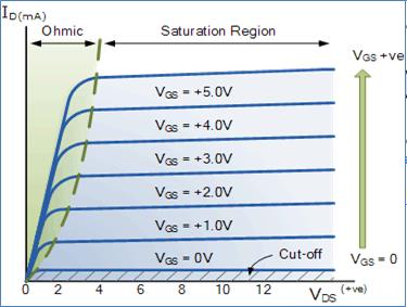
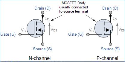
Enhancement-mode MOSFETs make excellent electronics switches due to their low “ON” resistance and extremely high “OFF” resistance as well as their infinitely high input resistance due to their isolated gate. Enhancement-mode MOSFETs are used in integrated circuits to produce CMOS type Logic Gates and power switching circuits in the form of a PMOS (P-channel) and NMOS (N-channel) gates. CMOS actually stands for Complementary MOS meaning that the logic device has both PMOS and NMOS within its design.


