Diode Construction
Diode Construction
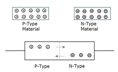
If a P-type and an N-type semiconductor material are attached to each other, and they form a PN junction.

As we already discussed P-type material has holes as the majority carriers and an N-type material has electrons as the majority carriers. As a result of PN junction opposite charges attract, few holes in P-type tend to move toward n-side and few electrons in an N-type move towards to P-side.
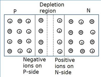
Both travels towards the junction, holes, and electrons recombine with each other to neutralize and form ions. At the junction, there exists a region where the positive and negative ions are formed, called a PN junction or junction barrier which form depletion region as shown in below figure.

As this region acts as a potential barrier between P and N-type materials, this is also called as Depletion region that’s mean depletes both the regions. There occurs a potential difference or voltage difference due to the formation of ions, across the junction so it is called as Potential Barrier as it restricts further movement of holes and electrons through the junction.


